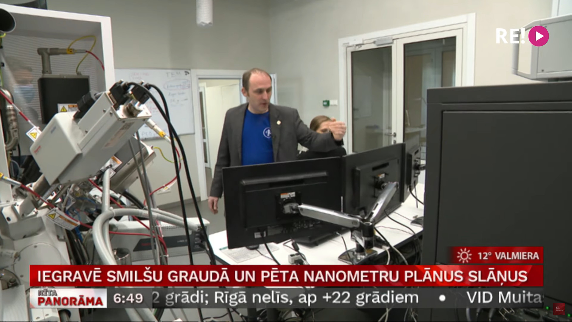
With the help of the scanning electron microscope, obtained within the scope of the ERDF project 1.1.1.4 to support CAMART2 project in terms of infrastructure development, scientists from the Laboratory of Materials Morphology and Structure Investigation can work with things as tiny as a nanometer or one-billionth part of a meter. The used scanning electron microscope Helios 5 UX is also an ion microscope and it is the best in Latvia and in the Baltic Sea countries.
On June 9, the head of the Laboratory of Materials Morphology and Structure Investigation, Dr.phys. Krišjānis Šmits in a story broadcasted by the National Television morning news program “Rīta Panorāma” explains that with such a special microscope it is possible not only to look at exceedingly small things, but also to engrave several letters, for example, in a grain of sand. However, at the laboratory they do no such things, because the microscope is used to check the thickness of the transistor layers to be inserted in mobile phone processors, which are usually about seven nanometers thin. With the help of a scanning electron microscope, it is also possible to investigate tiny layers of glasses that make them thin and clear, OLED lamps, antibacterial coatings, and many other new materials.
In the story, it is explained that ISSP UL cooperates with Latvian manufacturers so that they can offer competitive products to the world, which humanity will use in the future, probably without even realizing that everything is based on inventions that have originated in Latvia.
K. Šmits summarizes that a scientist should be a driving force and not someone who is told what to do. The scientist constantly makes decisions based on the achieved results and imagines what the result could be if something were done differently. Otherwise, the person is a good performer, but not a scientist.
The TV story in Latvian